The application of quartz glass plates in the electronic information industry
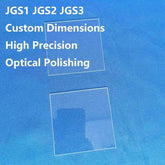
Quartz glass is a key strategic material that plays a crucial role in the electronic information industry. Its primary application areas are flat panel display devices and integrated circuit manufacturing, particularly in the field of high-precision photomask substrate preparation, where it plays an irreplaceable role. Quartz glass plates are an essential component for a number of high-end manufacturing technologies, including TFT-LCDs, OLED displays and advanced IC packaging. Their key characteristics, such as being ultra-high purity (SiO2 content can reach over 99.99%) and exhibiting excellent thermal stability and optical uniformity, make them the ideal supporting material for these sophisticated technological applications.

1. Domestic quartz glass plates are mainly applied in the following key fields:
(1) High-resolution display
It meets the precise requirement of TFT/OLED photomasks for a line width of less than 3 μm, thereby providing fundamental support for new display technologies.
(2) Miniaturized electronics
It is used in the field of MEMS (micro-electromechanical systems) and sensor manufacturing. Its primary function is to guarantee sub-micron-level graphic accuracy and to encourage the miniaturization development of electronic products.
(3) Advanced packaging
In BGA (ball grid array) and CSP (chip scale package) processes, microstructure processing below 5 μm is achieved in order to enhance the precision of the packaging technology.

2. Quality standards and technical challenges
The quality standards for quartz glass substrates are extremely strict, mainly including the following aspects:
(1)Zero-defect surface: In order to comply with the 50,000 lux detection light requirement, it is essential to ensure that no microscopic defects, such as cracks or bubbles, are present.
(2) Dimensional accuracy: It should comply with international standard systems, such as the 152×152×6.35mm (Model 6025) specification, as well as other relevant specifications.

(3) Nanoscale roughness: Ensuring the accuracy of pattern transfer in the photolithography process is of vital importance for high-end manufacturing.


